IoT SoC
This was the final project for EE140/240A, Linear Integrated Circuits, at UC Berkeley in Spring 2020.
Problem Overview
For a hypothetical mixed-signal chip which includes a microprocessor, flash and RAM memory, and several analog outputs and inputs, work as a group of three to design all of the analog components of this chip:
- 8-bit successive-approximation analog-to-digital converter (SAR ADC)
- Programmable-gain switched-capacitor amplifier (PGA)
- Bandgap voltage reference and temperature sensor (BGT)
- Analog multiplexer (MUX)
- Analog and digital voltage regulators (AREG,DREG)
The chip will be battery-powered, so the circuits need to operate properly from 3.2V down to 1.6V or less.1 It should meet all specifications over the industrial temperature range (-40 to +85 °C).
img hereAll of the circuit blocks share a common ground. Only the microprocessor runs off of VDDD, and all other blocks run off of either VDDA or VBAT. VDDD should be nominally 1.5V, and you may choose VDDA.
1
SAR ADC
Discuss design here
schematic
Results
| Cap DAC: Isolated Performance Error [LSB] | |||
|---|---|---|---|
| Temp [\(^{\circ}\)C]
Bit
|
-40 | 27 | 85 |
| 0 | 0.113 | 0.119 | 0.130 |
| 1 | 0.113 | 0.117 | 0.140 |
| 2 | 0.112 | 0.117 | 0.131 |
| 3 | 0.110 | 0.116 | 0.128 |
| 4 | 0.108 | 0.111 | 0.124 |
| 5 | 0.102 | 0.105 | 0.113 |
| 6 | 0.090 | 0.095 | 0.998 |
| 7 | 0.071 | 0.146 | 0.399 |
Discuss results here
programmable-gain amplifier
Discuss design here
schematic
Results
| PGA: Isolated Performance Average Error [LSB] | |||
|---|---|---|---|
| Temp [\(^{\circ}\)C]
Gain [V/V]
|
-40 | 27 | 85 |
| 1 | 4.5 | 4.89 | 9.34 |
| 2 | 3.11 | 2.55 | 4.76 |
| 3 | 2.24 | 1.64 | 4.1 |
| 4 | 2.59 | 2.01 | 4.05 |
| 5 | 1.3 | 0.96 | 3.55 |
| 6 | 1.78 | 1.48 | 4.05 |
| 7 | 0.83 | 0.46 | 3.26 |
| 8 | 2.27 | 1.90 | 4.68 |
| Mean | 2.33 | 1.99 | 4.72 |
Discuss results here
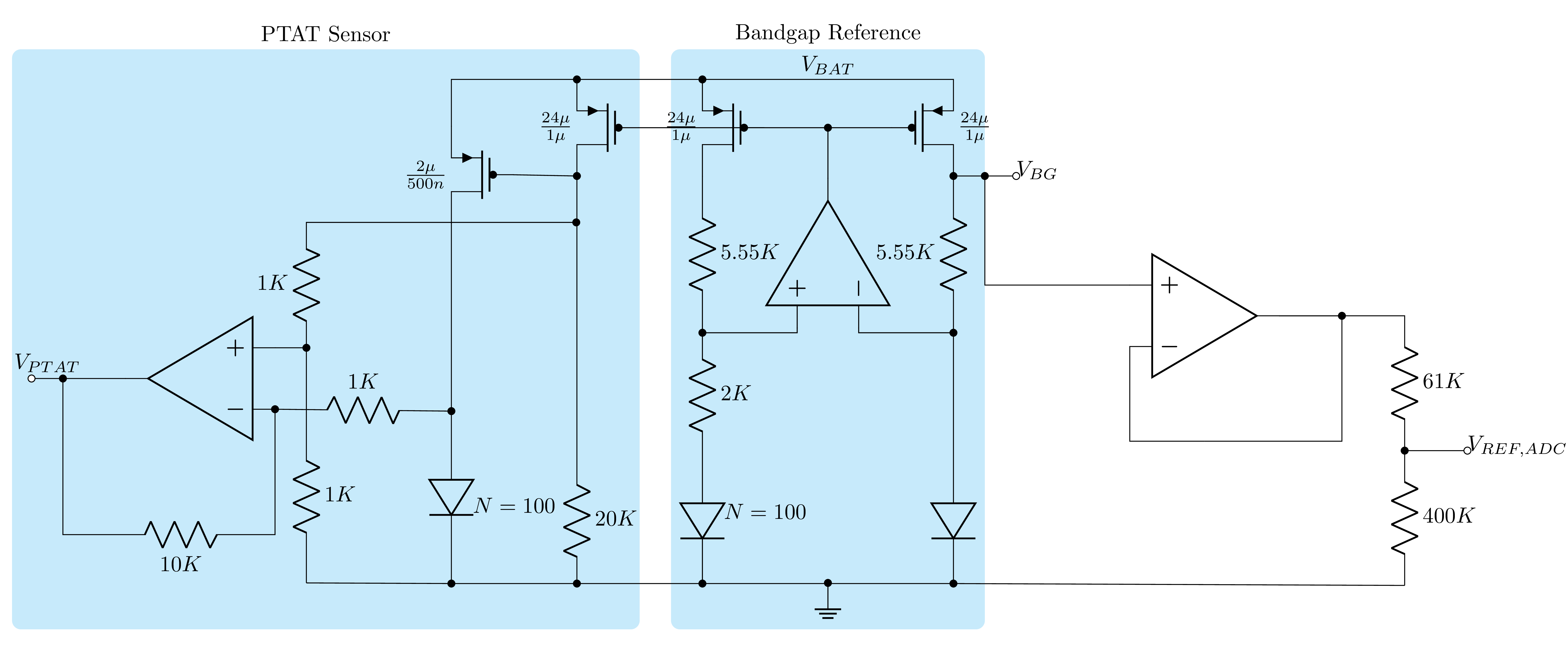
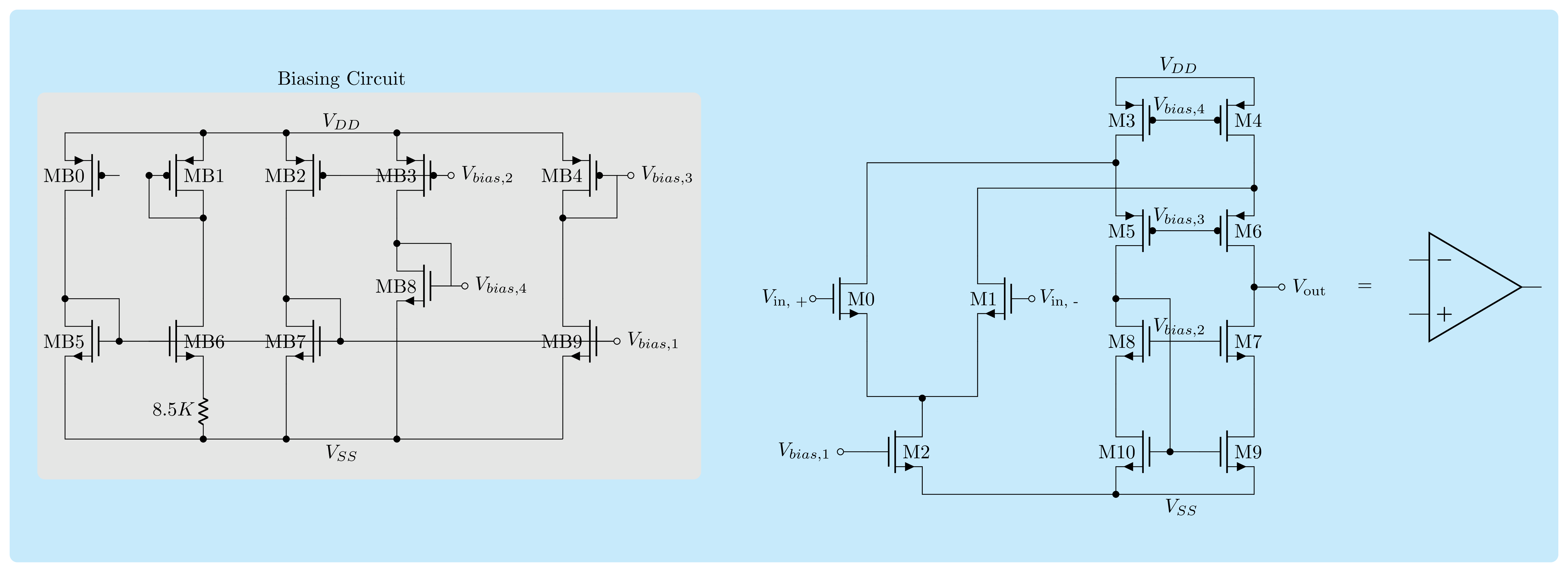
bandgap voltage reference
Discuss design here
schematic
Results
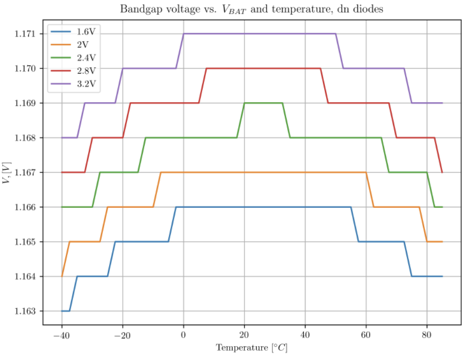
| \(V_{BG}\) Variation (% Error) | |||
|---|---|---|---|
| Temp [\(^{\circ}\)C]
\(V_{BAT}\) [V]
|
-40 | 27 | 85 |
| 1.6 | 0.7 | 1 | 1.12 |
| 2.4 | 0.5 | 0.4 | 0.6 |
| 3.2 | 0.7 | 0.5 | 1.2 |
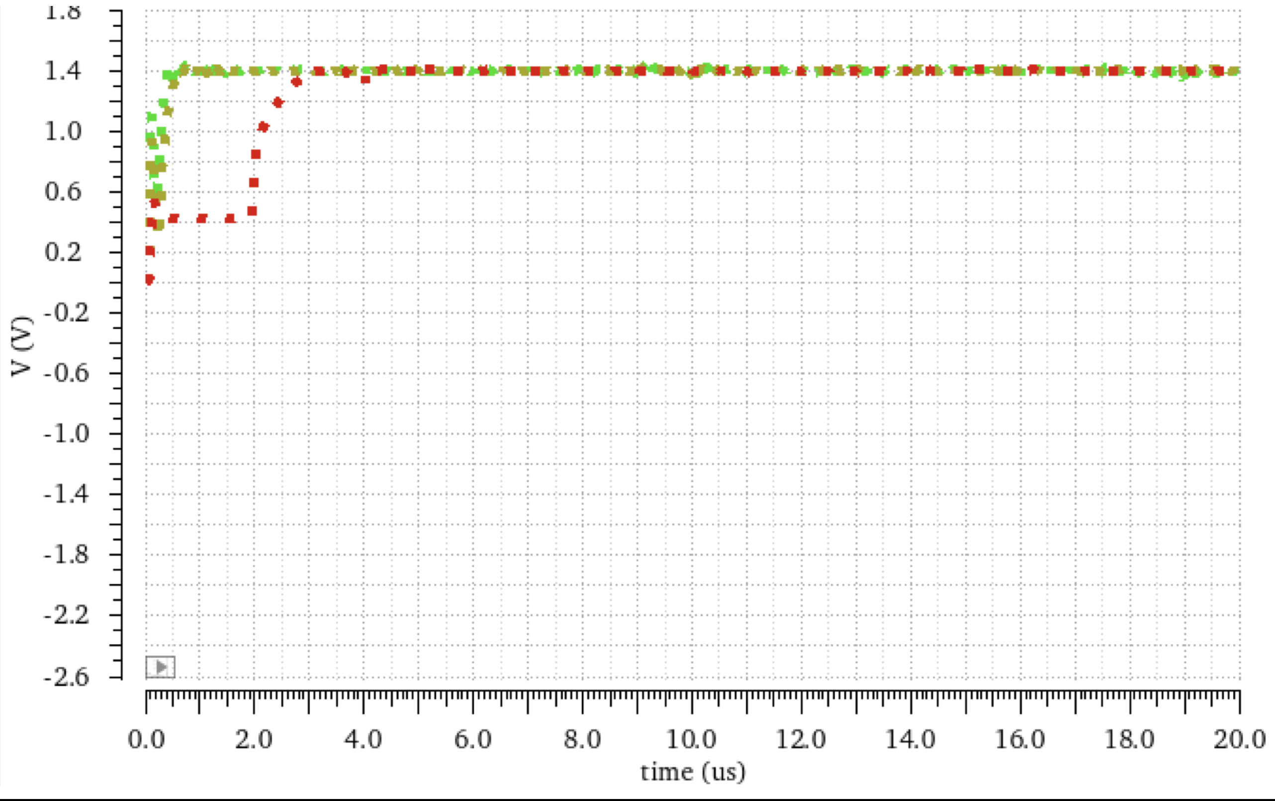
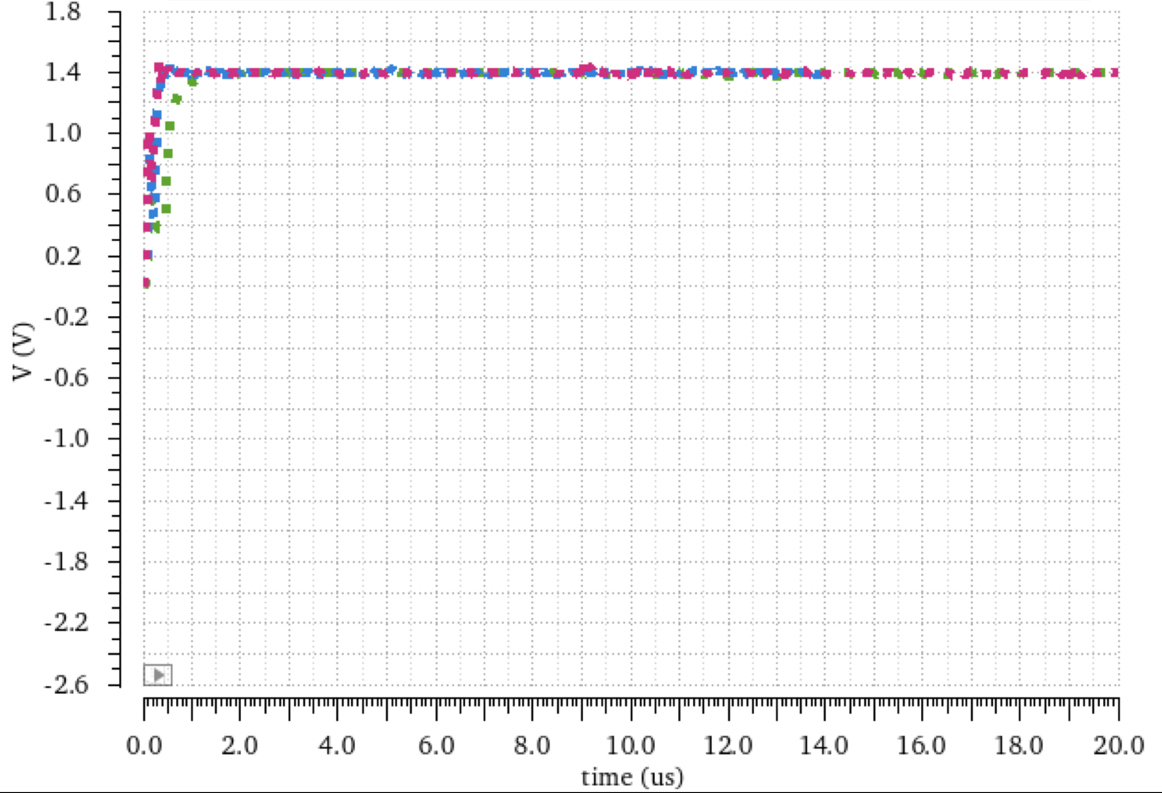
| Bandgap Transients | ||
|---|---|---|
| -40\(^{\circ}\)C | 27\(^{\circ}\)C | 85\(^{\circ}\)C |
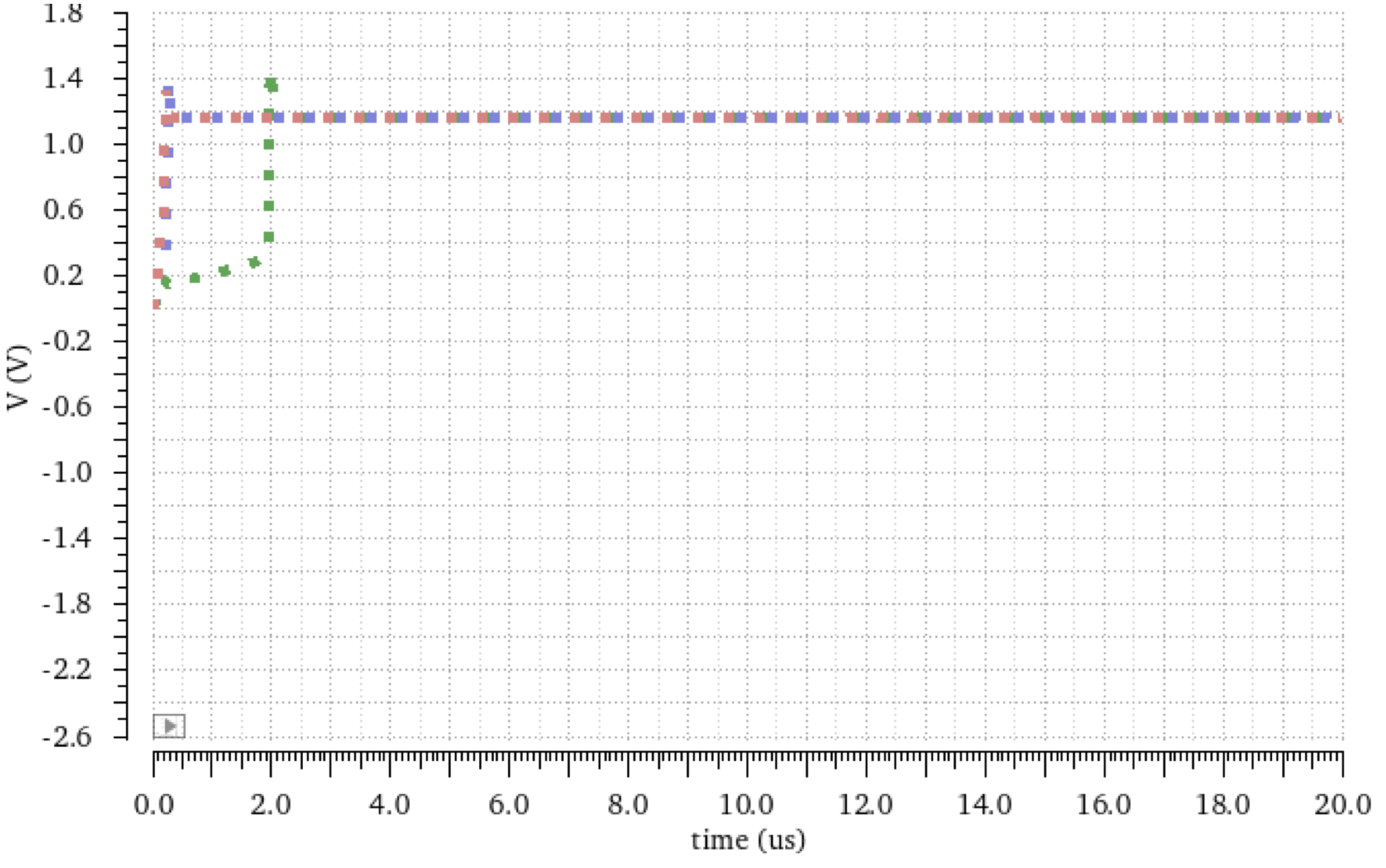 |
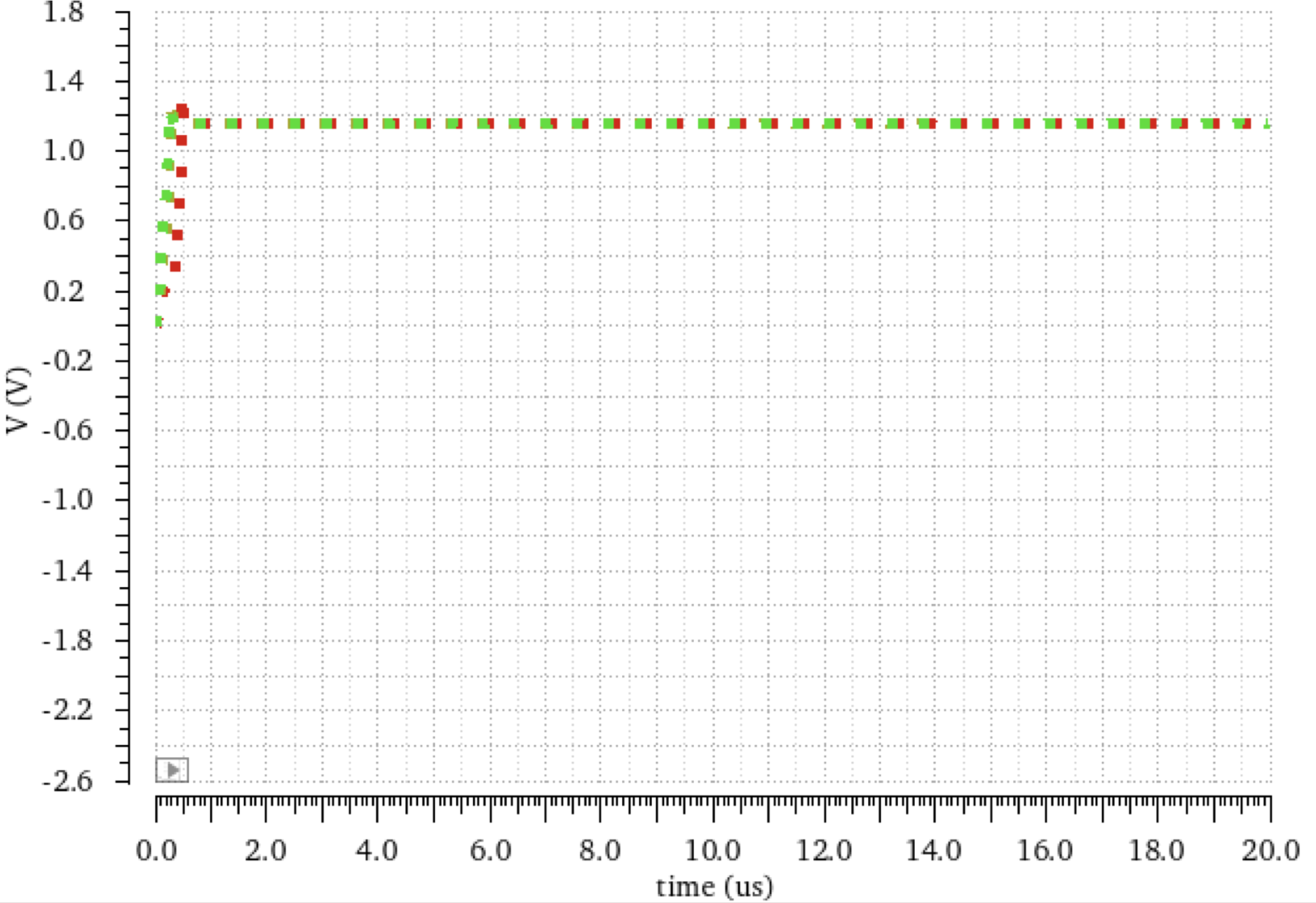 |
 |
| Bandgap Startup Time (\(\mu s\)) | |||
|---|---|---|---|
| Temp [\(^{\circ}\)C]
\(V_{BAT}\) [V]
|
-40 | 27 | 85 |
| 1.6 | 0.4 | 0.4 | 0.52 |
| 2.4 | 0.3 | 0.6 | 0.5 |
| 3.2 | 2.3 | 0.6 | 0.52 |
Discuss results here
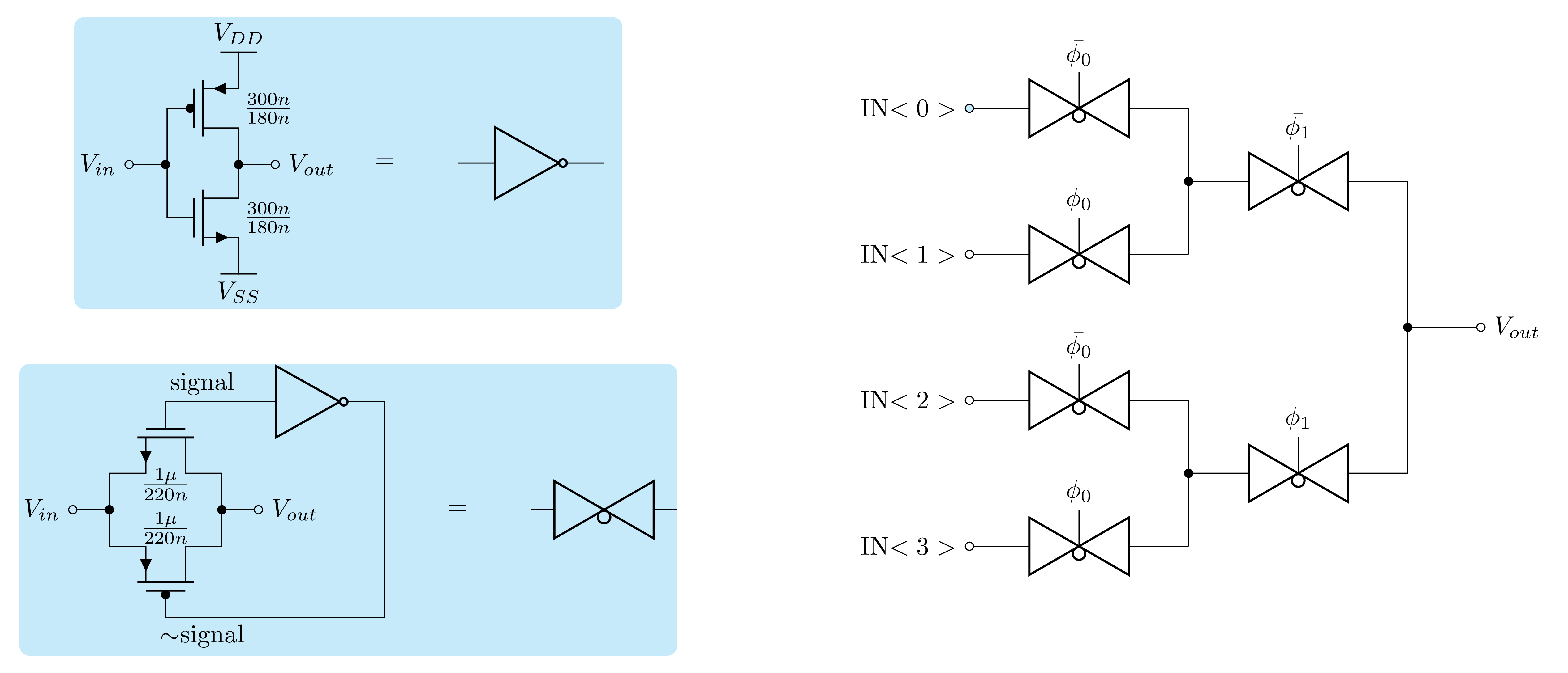
analog mux
Discuss design here
schematic
Results
| \(R_{on}\) vs. \(V_{in}\) | |
|---|---|
| Temperature \(^{\circ}\)C | Max \(R_{on}\) vs. \(V_{in}\) |
| -40\(^{\circ}\)C | 4136.7 \(\Omega\)/V |
| 27\(^{\circ}\)C | 5330 \(\Omega\)/V |
| 80\(^{\circ}\)C | 6313.3 \(\Omega\)/V |
Discuss results here
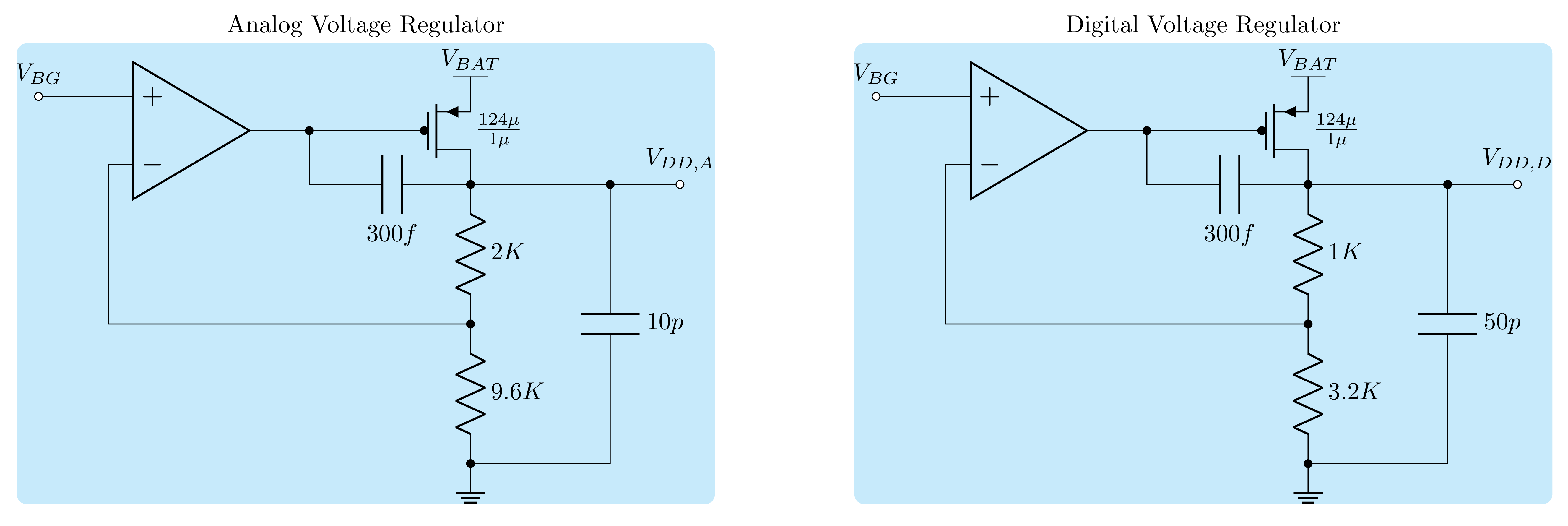
voltage regulators
Discuss design here
schematic
Results
| \(V_{DDA}\) Variation (% Error) | |||
|---|---|---|---|
| Temp [\(^{\circ}\)C]
\(V_{BAT}\) [V]
|
-40 | 27 | 85 |
| 1.6 | 0.8 | 0.8 | 7 |
| 2.4 | 0.6 | 3.5 | 6 |
| 3.2 | 0.7 | 1.2 | 7 |
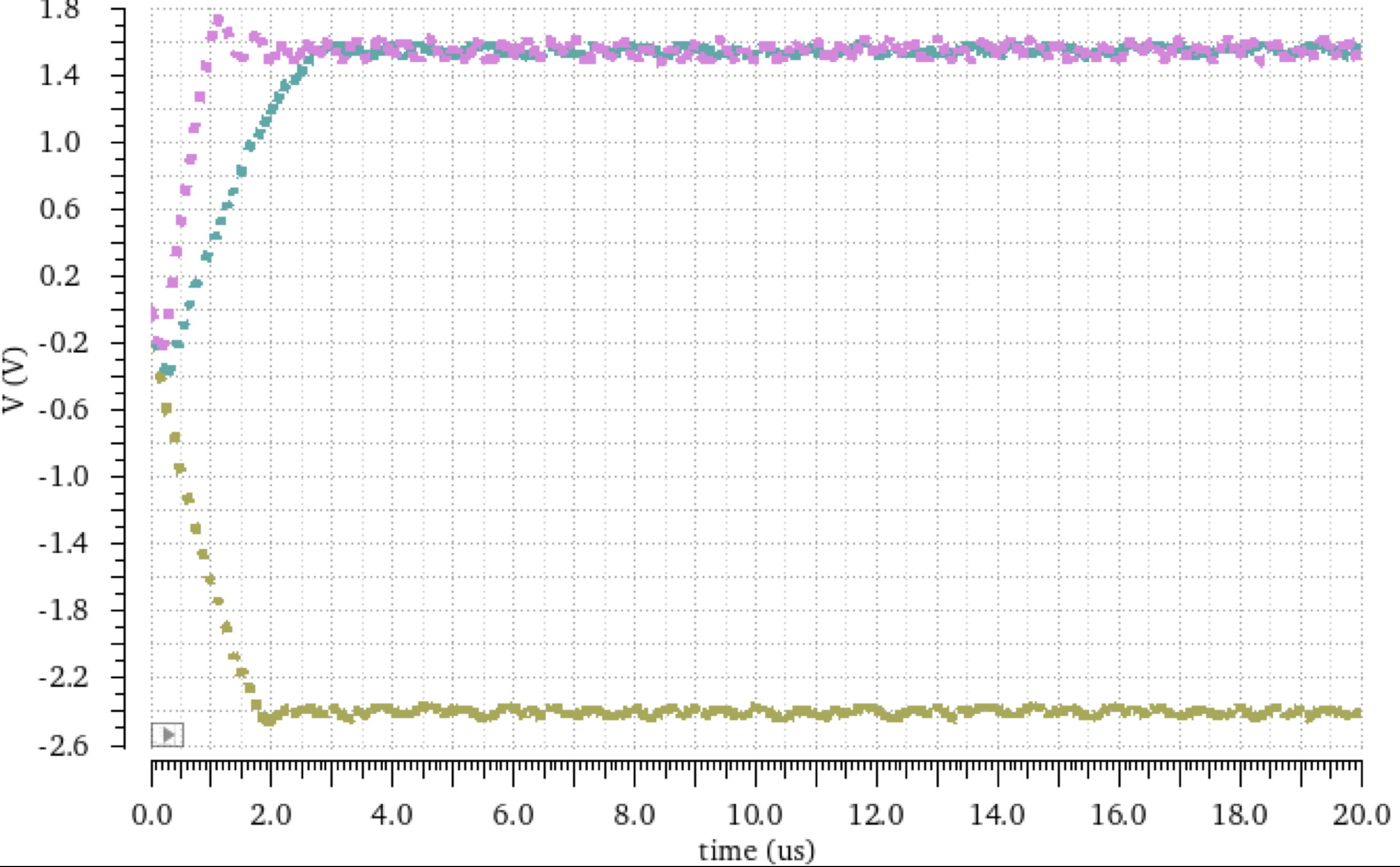
| AREG Transients | ||
|---|---|---|
| -40\(^{\circ}\)C | 27\(^{\circ}\)C | 85\(^{\circ}\)C |
 |
 |
|
| \(V_{DDD}\) Variation (% Error) | |||
|---|---|---|---|
| Temp [\(^{\circ}\)C]
\(V_{BAT}\) [V]
|
-40 | 27 | 85 |
| 1.6 | 230 | 230 | 230 |
| 2.4 | 3.3 | 4.6 | 4.6 |
| 3.2 | 1.3 | 6 | 34.6 |
| DREG Transients | ||
|---|---|---|
| -40\(^{\circ}\)C | 27\(^{\circ}\)C | 85\(^{\circ}\)C |
 |
 |
|
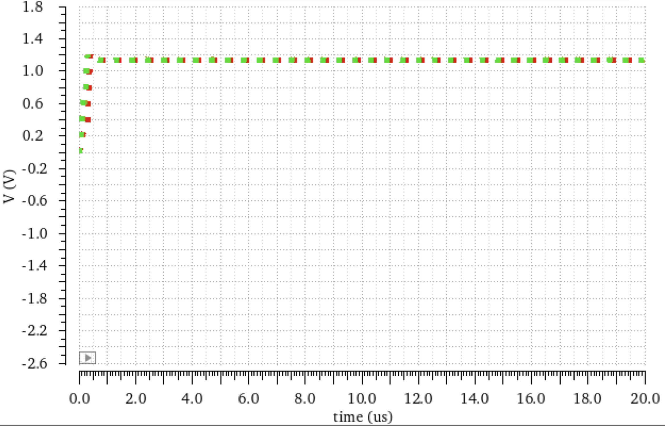
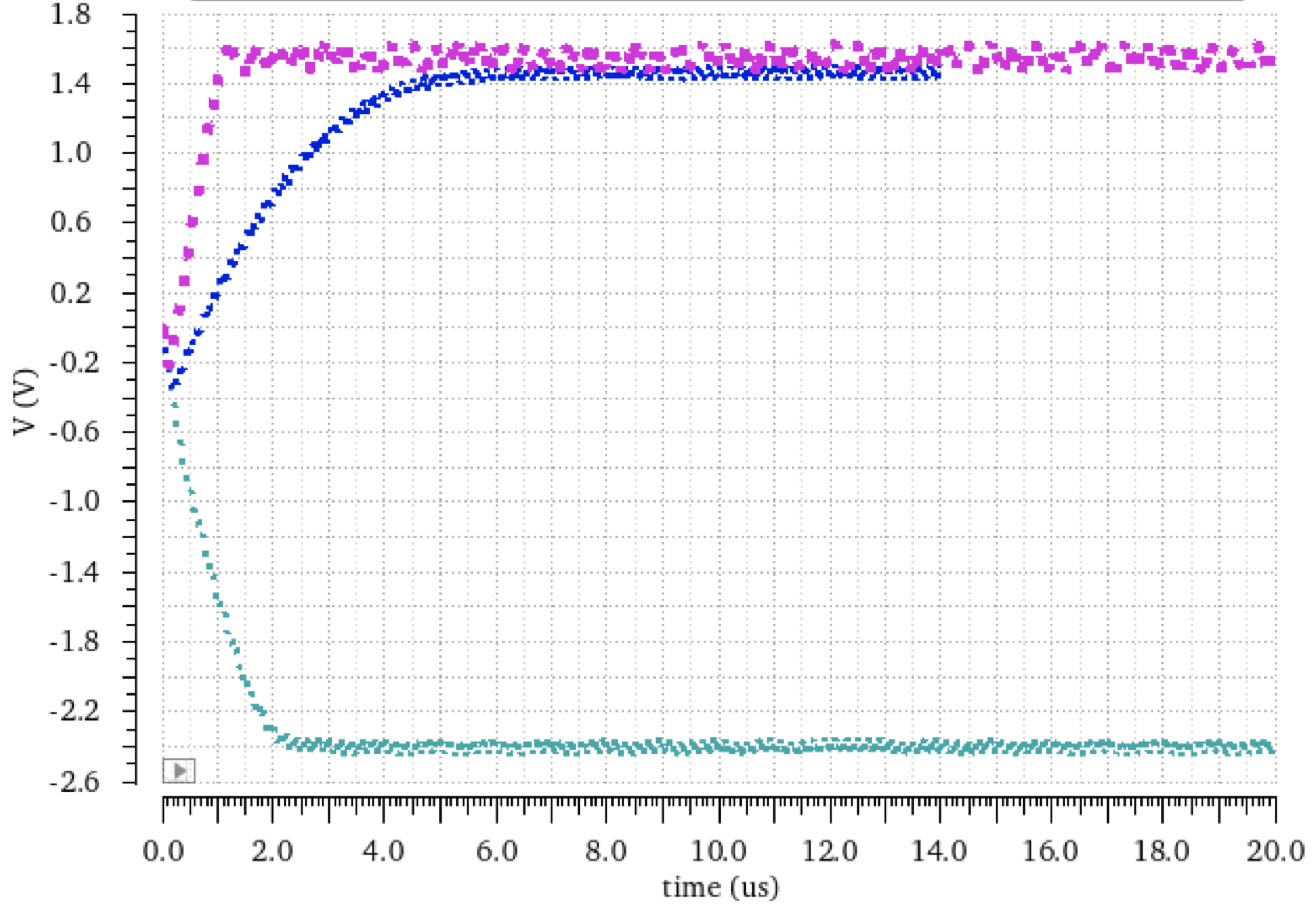
DREG Startup Failure
The transient data above was obtained from full-chip integrated simulation. The data demonstrate a DREG startup failure for low \(V_{BAT}\) which was not present in isolated and semi-integrated (with all components except ADC) simulation.
This failure was rectified by widening the DREG's output transistor from 124\(\mu\)m to 450 \(\mu\)m, as shown in the plot below, which was obtained from full-chip integrated simulation with \(V_{BAT} = 1.6V\) after widening the output transistor.
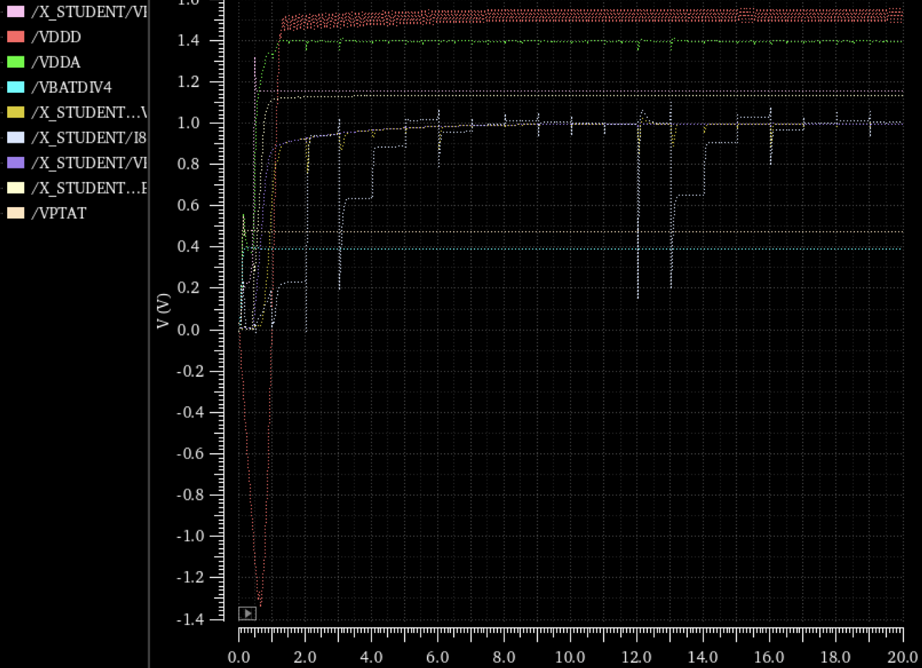
The x-axis in the figure is in units of \(\mu\)s.
Since running the full-chip integrated simulation for all gains and inputs took days, we were not able to retake all the data in time, so the remainder of the data shown in the overall results section are from the simulations prior to fixing the startup issue.
Power ConsumptionMaximum power consumption for the bandgap and regulators occurred at a temperature of 27\(^{\circ}\)C with \(V_{BAT} = 2.4V\).
- Bandgap: 0.6W
- AREG: 900 \(\mu\)W
- DREG: (max) 0.1W
Discuss results here
Overall Results
Area
Total Area: 1,049,820.896 \(\mu m^2\) (or 1.05 \(mm^2\))
Notable Contributors:
- BGR: 43.9%
- AREG: 24.1%
- PGA: 11.5%
- ADC: 11.0%
Resistors accounted for 81.1% of the total area. Since the bandgap reference and PTAT sensor used a significant number of resistors, including one with a value of 400K\(\Omega\), it makes sense that the BGR took up such a large portion of the chip area.
PowerThe chip pulled 227 mA with \(V_{BAT}\) at 3.2V, yielding a power consumption of 726 mW.
Startup Time: 10 \(\mu\)sTotal Cost: $0.13
Integration Error
| Average PGA Error, Gain=1 [LSB] | |||
|---|---|---|---|
| Temp [\(^{\circ}\)C]
\(V_{BAT}\) [V]
|
-40 | 27 | 85 |
| 1.6 | 1.34 | 0.518 | 1.33 |
| 2.4 | 4.03 | 2.52 | 9.99 |
| 3.2 | 6.89 | 3.18 | 19.1 |
| Average ADC Error, Gain=1 [LSB] | |||
|---|---|---|---|
| Temp [\(^{\circ}\)C]
\(V_{BAT}\) [V]
|
-40 | 27 | 85 |
| 1.6 | -- | -- | -- |
| 2.4 | 4.17 | 3.33 | 11 |
| 3.2 | 6.17 | 3.33 | 6 |
| Average PGA Error, Gain=2 [LSB] | |||
|---|---|---|---|
| Temp [\(^{\circ}\)C]
\(V_{BAT}\) [V]
|
-40 | 27 | 85 |
| 1.6 | -- | -- | -- |
| 2.4 | 3.29 | 2.31 | 3.66 |
| 3.2 | 5.25 | 3.63 | 7.25 |
| Average ADC Error, Gain=2 [LSB] | |||
|---|---|---|---|
| Temp [\(^{\circ}\)C]
\(V_{BAT}\) [V]
|
-40 | 27 | 85 |
| 1.6 | -- | -- | -- |
| 2.4 | 3.98 | 3.33 | 8.5 |
| 3.2 | 7 | 2.5 | 10.7 |
| Average PGA Error, Gain=3 [LSB] | |||
|---|---|---|---|
| Temp [\(^{\circ}\)C]
\(V_{BAT}\) [V]
|
-40 | 27 | 85 |
| 1.6 | -- | -- | -- |
| 2.4 | 3.91 | 1.59 | 7.69 |
| 3.2 | 2.51 | 1.74 | 12.8 |
| Average ADC Error, Gain=3 [LSB] | |||
|---|---|---|---|
| Temp [\(^{\circ}\)C]
\(V_{BAT}\) [V]
|
-40 | 27 | 85 |
| 1.6 | -- | -- | -- |
| 2.4 | 4 | 3.33 | 10 |
| 3.2 | 5.33 | 3.5 | 11 |
| Average PGA Error, Gain=5 [LSB] | |||
|---|---|---|---|
| Temp [\(^{\circ}\)C]
\(V_{BAT}\) [V]
|
-40 | 27 | 85 |
| 1.6 | -- | -- | -- |
| 2.4 | 2.10 | 2.64 | 5.75 |
| 3.2 | 3.97 | 3.11 | 8.21 |
| Average ADC Error, Gain=5 [LSB] | |||
|---|---|---|---|
| Temp [\(^{\circ}\)C]
\(V_{BAT}\) [V]
|
-40 | 27 | 85 |
| 1.6 | -- | -- | -- |
| 2.4 | 4.5 | 3.83 | 8 |
| 3.2 | 7.33 | 3.67 | 10.7 |
| Average PGA Error, Gain=7 [LSB] | |||
|---|---|---|---|
| Temp [\(^{\circ}\)C]
\(V_{BAT}\) [V]
|
-40 | 27 | 85 |
| 1.6 | -- | -- | -- |
| 2.4 | 3.52 | 4.37 | 6.56 |
| 3.2 | 6.92 | 3.55 | 9.24 |
| Average ADC Error, Gain=7 [LSB] | |||
|---|---|---|---|
| Temp [\(^{\circ}\)C]
\(V_{BAT}\) [V]
|
-40 | 27 | 85 |
| 1.6 | -- | -- | -- |
| 2.4 | 2.67 | 3.33 | 7.67 |
| 3.2 | 6.83 | 4 | 8.67 |
| Average PGA Error, Gain=8 [LSB] | |||
|---|---|---|---|
| Temp [\(^{\circ}\)C]
\(V_{BAT}\) [V]
|
-40 | 27 | 85 |
| 1.6 | -- | -- | -- |
| 2.4 | 3.44 | 3.15 | 4.72 |
| 3.2 | 6.96 | 5.06 | 4.94 |
| Average ADC Error, Gain=8 [LSB] | |||
|---|---|---|---|
| Temp [\(^{\circ}\)C]
\(V_{BAT}\) [V]
|
-40 | 27 | 85 |
| 1.6 | -- | -- | -- |
| 2.4 | 4.94 | 3.00 | 5.83 |
| 3.2 | 6.50 | 4.50 | 8.17 |